Written by: Rita
The Hot Chips 2026 conference conveyed a clear signal: the rules of the AI chip race are changing.
On August 31, Barclays released a conference report highlighting that the core theme this year is no longer "who has the strongest computing power," but "who can do the most with the least electricity." Token/watt (the number of tokens produced per watt of electricity) has become the most critical metric for measuring the success of AI hardware. With both physical space and power supply in data centers being limited, hardware vendors, hyperscale manufacturers, and component suppliers are all emphasizing the same goal: to extract the maximum system performance within a fixed power budget. Barclays believes that the industry is shifting from pursuing peak performance of single chips to optimizing the system efficiency of entire racks, a change that will redefine the competitive landscape of AI hardware.
Token/watt replaces computing power as the top priority
Multiple speeches at the conference repeatedly emphasized a core logic: data center power supply is no longer a question of "what if it's not enough, just expand," but rather "with only this many watts, how many tokens can you produce."
AMD has made several optimizations to its accelerators, including enhancing the beyond function engine and increasing tensor data transport units, to improve computational efficiency per unit of power consumption. Microsoft has introduced a software-defined local access data stream (SDLA) architecture that improves energy efficiency while reducing total ownership costs through explicit software orchestration and the separation of data and control flows.
Barclays pointed out that this optimization pressure is being transmitted down through the entire hardware stack, from computation cores to memory architectures, from chip interconnects to packaging designs, with every link needing to pursue extreme efficiency within a limited power budget.
Inference workload partitioning becomes a key architectural divergence
The industry is currently experiencing profound divergence in the way inference workloads are partitioned. The traditional approach is to use different chips for training and inference, with the latest chips used for training and older products relegated to inference. Now, inference itself is being further split.
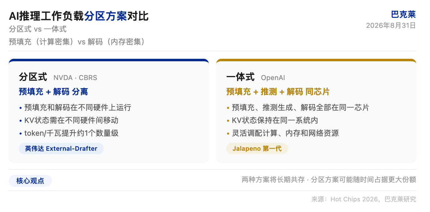
The most mainstream approach is to separate pre-filling (computationally intensive) and decoding (memory intensive) to run on different hardware. Nvidia showcased the External-Drafter speculative decoding solution at the conference, where a front model generates candidate tokens, which are then validated and confirmed by the main model. Cerebras is also pursuing inference partitioning, separating pre-filling and decoding, and has established partnerships with AMD and AWS. Barclays estimates that these solutions can provide an order of magnitude improvement in the token/kilowatt metric.
OpenAI has chosen the opposite path. Its Jalapeno chip completes pre-filling, speculative generation, and decoding all on the same chip. OpenAI's logic is that partitioning solutions require moving KV states between different hardware, which is less efficient than keeping KV within the same system and flexibly allocating computational, memory, and networking resources based on inference step requirements.
Barclays believes both solutions will coexist, and different AI labs and hyperscale vendors will ultimately adopt a variety of solutions. Jalapeno is just the first generation product; over time, partitioning solutions may occupy a larger share.
ASIC ecology trends towards diversification and system-level competition
Hyperscale vendors' ASICs are expanding from targeting specific use cases (such as Meta's advertising recommendation system) to more general Agentic AI solutions. Chip designs are covering a broader range of problem domains, thereby achieving wider applicability.
Competition is extending from individual computing modules to entire infrastructure layers. Each ASIC solution is enhancing system-level performance through unique interconnect topologies and memory configurations. Differentiation in interconnects and memory is becoming a new competitive focus.
Google's TPU has introduced MediaTek as a second supplier while also incorporating Marvell into a variant of its inference solution. Barclays assesses that the current TPU still relies on Broadcom as its "main plan," but the COT (customer-owned tools) model will gain more attention in the second half of 2026.
OpenAI's Jalapeno chip went from initial RTL to tape-out in just nine months, with the engineering team stating that most of its IP was developed from scratch. While Barclays is unclear on Broadcom's level of involvement in core design, the accumulations of Broadcom and Marvell in SerDes and supply chain capabilities still provide significant value in ASIC mass production.
Base die customization and 3D DRAM lead memory innovation
The capacity, bandwidth, and power consumption of memory are another core topic of this conference. Nvidia's NVHBM plan will move customized memory controllers from XPU chips to the HBM base die. This improvement is expected to deliver up to a 30% increase in memory bandwidth, a 15% decrease in HBM power consumption, and free up 25% of the area on XPU computation chips.
The central debate is about who holds the dominant control over customization. Memory has long been viewed as a commodity, but customized solutions will make XPU designers more reliant on single memory suppliers. Barclays tends to believe that the ultimate control will lie with accelerator companies rather than memory manufacturers, as accelerator companies need to maintain flexibility with multiple supply sources.
3D DRAM is another emerging direction. Samsung's zHBM solution is currently under exploration, and Cerebras plans to adopt hybrid bonding technology in its CS-6. These solutions have the potential to significantly enhance power efficiency and overall bandwidth, but thermal management and power supply remain major challenges in the early stages.
CXL memory expansion is also worth noting. Barclays has a cautious stance on previous CXL promotions, but the signals of industry demand at this conference should not be ignored. The first wave of use cases is expected to focus on memory expansion, followed by eventual evolution towards memory pooling.
The AI chip race has transitioned from the "peak computing power" phase to the "energy efficiency optimization" phase. Token/watt has replaced FLOPS as the benchmark; inference partitioning has become a key architectural choice; ASIC competition has extended to system-level differentiation; and memory customization and 3D stacking are rewriting the rules of the game. When every watt must be carefully calculated, those who can make optimal trade-offs at the system level will gain an advantage in the next phase.

Disclaimer
This article is an organization and interpretation of a third-party brokerage research report (Barclays, August 31, 2026) by ChaoXiang Research, combined with the organization of publicly available market information. The ratings, target prices, earnings forecasts, and related judgments quoted herein are opinions of the analysts at that brokerage and represent the position of their respective organizations, not the views of ChaoXiang Research, and do not constitute any investment advice.
The market has risks; decisions should be independent. This article should not be used as the basis for buying or selling any securities.
免责声明:本文章仅代表作者个人观点,不代表本平台的立场和观点。本文章仅供信息分享,不构成对任何人的任何投资建议。用户与作者之间的任何争议,与本平台无关。如网页中刊载的文章或图片涉及侵权,请提供相关的权利证明和身份证明发送邮件到support@aicoin.com,本平台相关工作人员将会进行核查。


